Difference between revisions of "GL128S11DHV02"
Jump to navigation
Jump to search
(Created page with "Flash ID: 02 00 7D 22 @ AAA/A9 Swapped pins: (0, 1) Device size: 0x1000000 (16.00 MB) Voltage: 2.7–3.6 V Single write: True Buffered write: True (512 Bytes) Chip erase...") |
Lesserkuma (talk | contribs) m |
||
| (3 intermediate revisions by the same user not shown) | |||
| Line 1: | Line 1: | ||
| − | Flash ID: 02 00 7D 22 @ | + | == Information == |
| + | ;Flash ID: 02 00 7D 22 | ||
| + | ;Device size: 0x1000000 (16.00 MB) | ||
| + | ;Voltage: 2.7–3.6 V | ||
| + | ;Single write: True | ||
| + | ;Buffered write: True (512 Bytes) | ||
| + | ;Chip erase: 32768–262144 ms | ||
| + | ;Sector erase: 256–2048 ms | ||
| + | ;Top/Bottom flags: 0x04 | ||
| + | ;Region 1: 0x0000000–0x0FFFFFF @ 0x20000 Bytes × 128 | ||
| − | Swapped pins: (0, 1) | + | == Cartridges with this chip == |
| − | + | <gallery widths=400 heights=300> | |
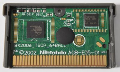
| − | + | File:BX2006_TS0P_64BALL - GL128S11DHV02 (Wario Land 4).jpg|''Repo cartridge of Wario Land 4 (patched for Flash ROM saving)''<br>'''PCB text:''' BX2006_TSOP_64BALL, © 2002 Nlhtehdo<br>'''Max. ROM size:''' 16 MB<br>'''Flash ID command:''' AAA/A9<br>'''Swapped pins:''' (0, 1) | |
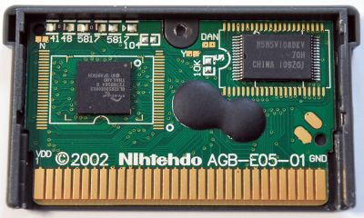
| − | + | File:AGB-E05-01 - GL128S90DHI02 (Pokémon Liquid Crystal).jpg|''Repo cartridge of Pokémon Liquid Crystal (fan game, patched for Flash ROM saving)''<br>'''PCB text:''' AGB-E05-01, © 2002 Nlhtehdo<br>'''Max. ROM size:''' 16 MB<br>'''Flash ID command:''' AAA/A9<br>'''Swapped pins:''' (0, 1)<br>''Flash chip is a variant (GL128S90DHI02)'' | |
| − | + | </gallery> | |
| − | |||
| − | |||
| − | |||
| − | |||
| − | |||
| − | |||
| − | |||
| − | |||
| − | |||
| − | |||
| − | |||
| − | |||
Latest revision as of 12:26, 2 December 2020
Information
- Flash ID
- 02 00 7D 22
- Device size
- 0x1000000 (16.00 MB)
- Voltage
- 2.7–3.6 V
- Single write
- True
- Buffered write
- True (512 Bytes)
- Chip erase
- 32768–262144 ms
- Sector erase
- 256–2048 ms
- Top/Bottom flags
- 0x04
- Region 1
- 0x0000000–0x0FFFFFF @ 0x20000 Bytes × 128

